Development of a high output 100mW DFB laser diode chip
- Responding to increasing data traffic and requirement for power consumption reduction within data centers -
September 16, 2022
- Furukawa Electric has successfully developed a DFB laser diode chip with an industry leading 100mW output power.
- This is in response to demand for increased optical transceiver performance at data centers.
- Higher output power contributes to reducing optical transceiver and data center power consumption.
Background
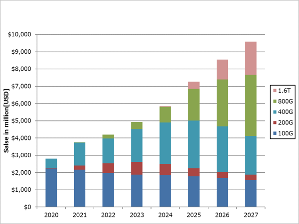
The performance of optical transceivers continues to increase along with the growth in data traffic. The former transmission speed was 400Gbps, but this is increasing to speeds exceeding 800Gbps, up to 1.6Tbps (Fig. 1). As transmission speed increases, the optical loss during high-speed, high-intensity modulation rises, making it necessary to have a DFB laser diode chip with increased output power. At the same time, the use of optical transceivers and other devices in the network equipment at data centers and network base stations has increased, and the growing power consumption is becoming an important issue.
Details
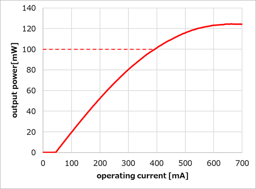
Using InP (Indium Phosphide, note 2) semiconductor chip technology experience accumulated over the years, we have successfully developed a DFB laser diode chip with high output power of 100mW - one of the highest in the world (Fig. 2). Through this new advancement, it will be possible to realize high performance optical transceivers that support at least 800Gbps large volume data communication, as well as respond to further growth in overall data traffic. Also, the creation of high performance transceivers using our high output power DFB laser diode chip as a key component should limit power consumption by the optical transceiver and reduce overall power consumption at the data center.
We plan to exhibit this new product at the European Conference on Optical Communication 2022 (ECOC 2022) scheduled to be held in Basel, Switzerland from September 19-22.
Main product specifications
| Characteristic | Specification | Characteristic | Specification |
|---|---|---|---|
| Optical output power |
100mW | Side mode suppression ratio |
Min. 35dB |
| Operating temperature |
-5 ~ +75℃ | Beam divergence angle (vertical) |
Typ. 22 deg |
| Peak wavelength |
1271/1291/1311/1331nm | Beam divergence angle (horizontal) |
Typ. 18 deg |
-
note 1Silicon photonics technology: Forming technology for high density optical device integrated platforms based on silicon electronics manufacturing technology. The ability to use widely adopted silicon electronics manufacturing technology makes it possible to reduce costs and achieve higher integration.
-
note 2InP (Indium Phosphide): A III-V semiconductor family that is used in the manufacturing of laser diode chips and high-speed transistors.
Furukawa Electric Group’s efforts towards the SDGs
Based on the “Sustainable Development Goals (SDGs)” adopted by the United Nations, Furukawa Electric Group has formulated the “Furukawa Electric Group Vision 2030” which sets the year 2030 as its target and is advancing efforts with the aim to “Build a sustainable world and make people’s life safe, peaceful and rewarding, Furukawa Electric Group will create solutions for the new generation of global infrastructure combining information, energy and mobility.” Toward the achievement of our Vision 2030, we will take open, agile, and innovative approaches to promote ESG management that aims to increase corporate value over the medium to long term and will contribute to the achievement of the SDGs.
The information contained in news releases is current at the time of release.
Please note that information regarding specifications, prices and service content, etc., are subject to change without notice.